Note: This post is translated and adapted from a VOA Chinese feature report originally titled “A Top Peking University Graduate Drives Chip Materials Innovation in the U.S.”
A Top Peking University Graduate Drives U.S. Chip Materials Innovation
By Fang Bing
Researchers at the Massachusetts Institute of Technology (MIT) have recently completed a cutting-edge technology that could help break through the limits of manufacturing more powerful semiconductor chips. Leading this technological innovation is a Chinese PhD student studying at MIT.
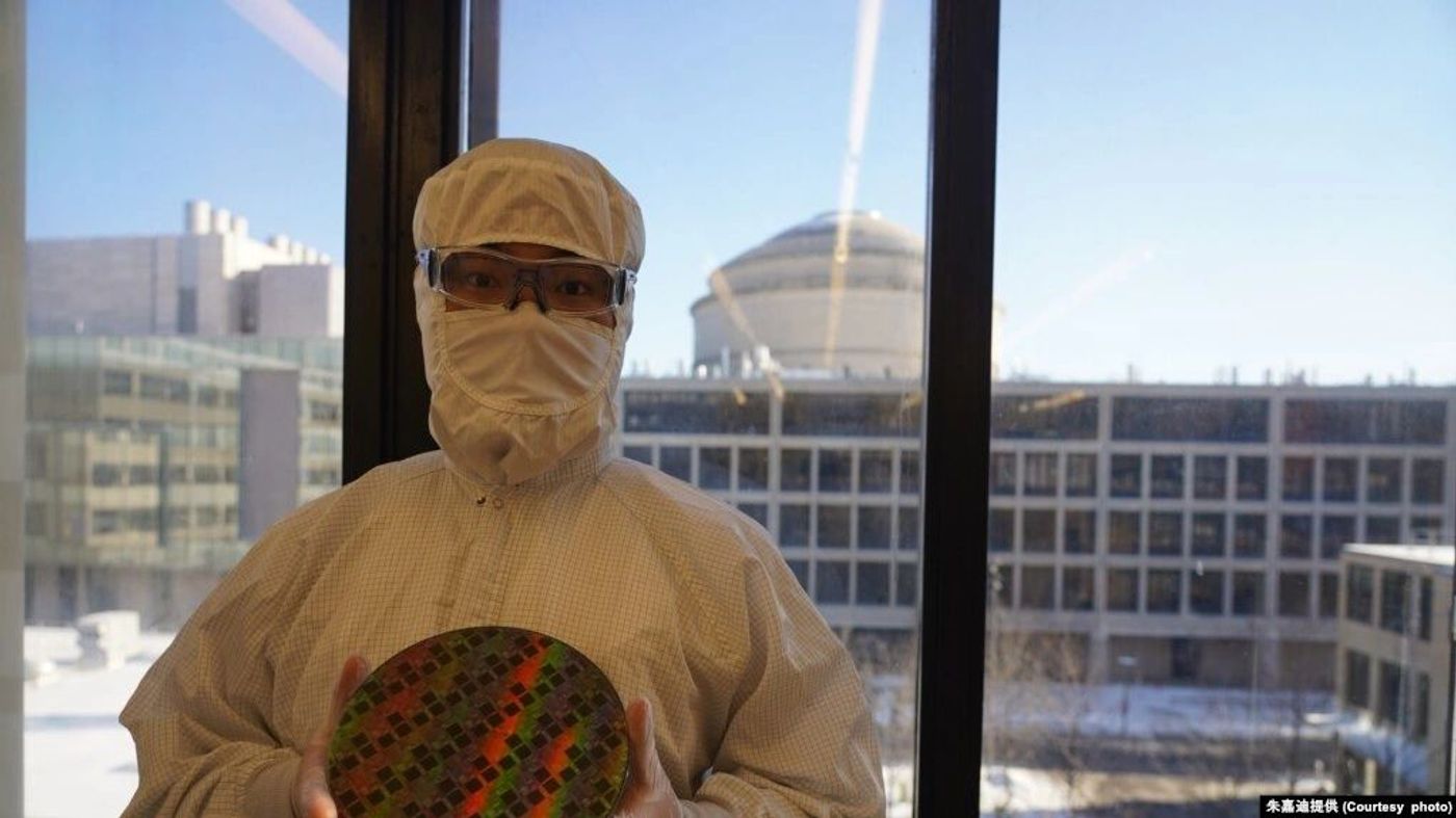
That student is 27-year-old Jiadi Zhu.
“I was born in Nanjing, attended the Nanjing Normal University High School, then went to Peking University for my undergraduate studies, and later came to MIT. I’m now a PhD student entering my fifth year,” Zhu told Voice of America. He is currently pursuing a doctorate in Electrical Engineering and Computer Science at MIT.
Emerging artificial intelligence applications require denser and more powerful computing chips. Traditionally, chips are made from bulk materials with three-dimensional structures. However, stacking multiple layers of transistors to achieve higher integration density — and therefore more powerful chips — has become increasingly difficult.
This challenge relates to Moore’s Law in chip manufacturing: the observation that chip performance doubles approximately every 18 to 24 months as transistor density increases. Today, advanced chip manufacturing is approaching the physical limits of dimensional scaling.
The research team coordinated by Zhu developed a new technology that allows two-dimensional material transistors to be directly grown on top of an 8-inch silicon wafer, enabling denser integration.
A paper describing the technology was published on April 27 in Nature Nanotechnology, with Zhu and MIT postdoctoral researcher Ji-Hoon Park as co-lead authors. Their achievement has been described as having the potential to extend — or even surpass — Moore’s Law.
Innovation in Materials, Design, and Processing
Zhu explained that their innovation primarily focuses on the first three of five key areas in chip manufacturing: materials, design, and processing (the remaining two being packaging and testing).
“Silicon has been used for nearly 60 years and is approaching its limits,” Zhu said. “We developed a large-scale, high-quality supply method for single-layer molybdenum disulfide across an 8-inch wafer. This significantly increases the available material scale.”
To explain the design concept, Zhu used a housing analogy:
“A single-story house can only accommodate a few people. But if you build a multi-story building, you can hold many more.”
Traditional silicon circuits are like single-story structures — single-layer circuits. The new approach enables a monolayer sulfide semiconductor to be directly synthesized or deposited on top of existing silicon circuits. Using two-dimensional molybdenum disulfide materials makes heterogeneous integration feasible.
In processing, the team developed a low-temperature fabrication method that allows additional layers to be added without damaging the underlying circuits.
Zhu entered MIT in 2019. He said the entire innovation forms the core topic of his doctoral dissertation. “It’s essentially a semi-assigned research direction — your advisor defines a broad direction when you first arrive.”
When asked what the innovation means for future advanced chip nodes such as 1-nanometer manufacturing, Zhu explained that the “1 nm” label is largely symbolic.
“At the 1-nanometer node, nothing is actually one nanometer,” he said. “Below the 28-nanometer technology node, these labels are technical indicators. They represent roughly a doubling of chip performance per unit area compared to the previous generation.”
Enabling More Advanced Chip Manufacturing
At 1-nanometer or more advanced nodes, Zhu said their materials innovation increases integration density through vertical stacking.
“If scaling the first layer becomes stuck — because the smallest physical dimension at the 1-nanometer node is about 12 nanometers — and lithography struggles to pattern features smaller than that, then you can build upward,” Zhu explained. “You can stack many layers.”
Two-dimensional materials provide a viable system for such stacking. Additional layers can be built on top of silicon using existing lithography tools while maintaining precision at around 12 nanometers per layer, ultimately achieving high-density integration.
“This is the significance of our work,” Zhu said. “Beyond continued scaling, the future lies in further stacking and 3D integration. And this heterogeneous integration approach is also applicable to mature, larger technology nodes.”
However, Zhu emphasized that applying the technology to industrial mass production still requires additional steps.
“We address the first three stages,” he said. “Packaging and testing remain equally critical.”
Some Chinese media quoted experts saying the achievement is “not a disciplinary breakthrough” and should be viewed primarily as an academic paper, noting that domestic scientists have already demonstrated sub-1-nanometer gate-length transistors using monolayer molybdenum disulfide.
Zhu said this interpretation reflects a misunderstanding.
“What we achieved is wafer-scale growth, low-temperature growth, and direct heterogeneous integration. This had not been done successfully before at the 8-inch wafer scale,” he said. “Our work significantly advances integration, and companies are already showing strong interest.”
Geopolitical Constraints on Scientific Research
Semiconductors have become a focal point of geopolitical competition between the United States and China. The Biden administration has imposed sweeping export controls on advanced chips to China. Chinese President Xi Jinping has called this an attempt to “choke” China’s development and has vowed technological self-reliance while taking countermeasures against U.S. memory chip maker Micron.
“There are definitely restrictions,” Zhu said regarding today’s research environment. “Even normal academic collaborations can raise concerns. Sometimes, for safety reasons, projects are paused or not pursued. That is a real worry.”
A June study published in the Proceedings of the National Academy of Sciences surveyed 1,304 Chinese American scientists and found many feel unsafe conducting research, collaborating with China, or applying for federal funding.
In 2021, MIT professor Gang Chen, director of the university’s micro-nano engineering lab, was arrested under the U.S. Justice Department’s “China Initiative.” Charges were dropped a year later after prosecutors concluded he had no obligation to disclose certain affiliations.
The case triggered strong protests from the academic community and Asian American groups, who argued Chen was targeted because of his ethnicity. The Justice Department formally ended the China Initiative in 2022.
Zhu said MIT remains a positive environment.
“The university provides equal protection and support for everyone,” he said.
Debate Over Talent Migration
News of Zhu’s work sparked intense discussion on Chinese social media. Some commentators lamented that Chinese talent contributes to U.S. technological advancement.
Zhu said such narratives do not reflect his personal experience.
“I feel that many of the stories promoted by domestic self-media have little to do with me,” he said. “I want to find a place that needs me and allows me to grow. Such environments exist in both China and the United States.”
Zhu noted that he received Peking University’s prestigious May Fourth Medal — one of the university’s highest student honors — awarded to roughly 100 recipients over two decades across undergraduate, master’s, and doctoral levels.
He credited Peking University with strong mentorship and academic resources. As an undergraduate, he published in leading journals including Advanced Materials and IEEE Electron Device Letters.
“I don’t feel there’s a huge difference between Peking University and MIT,” Zhu said. “If there is one, it’s in research culture and habits, not capability. This has been a valuable learning experience, and it’s an academic journey unrelated to politics.”
Asked about his plans after completing his PhD, Zhu said the decision will depend on personal ambition, career platform, and family considerations.
“I hope to align these factors,” he said.
MIT PhD student Jiadi Zhu holding an 8-inch wafer. (Courtesy of Jiadi Zhu)